
 |
A/D Converter Makers
Address Signaling Noise Issues With LVDS Output Converters
By Bettyann
Liotta, eeProductCenter
Oct 15 2004 (12:49 PM)
URL: http://www.eeproductcenter.com/showArticle.jhtml?articleID=49901582

Why LVDS Outputs Are Needed
Analog-to-digital converter (A/D
converter) sample rates have been increasing steadily for years to accommodate
newer bandwidth hungry applications in communication, instrumentation, and
consumer markets. Coupled with the need to digitize signals early in the signal
chain to take advantage of digital signal processing techniques, this has
motivated the development of high-speed A/D converter cores that can digitize at
greater than 100 MHz to 200 MHz clock rates with 8-to 12-bit resolution. In
standalone converters, the A/D converter needs to be able to drive receiving
logic and accompanying printed-circuit board trace capacitance. Current
switching transients due to driving the load can couple back to the A/D
converter analog front end, adversely affecting performance. One approach to
minimize this effect has been to provide the output data at one-half the clock
rate by multiplexing two output ports, reducing required edge rates, and
increasing available settling time between switching instants.
Another approach to providing high-speed data outputs while minimizing performance limitations in A/D converter applications is the use of low voltage differential signaling (LVDS). Many A/D converter makers, including Analog Devices Inc., Linear Technology Corp., Maxim Integrated Products, National Semiconductor Corp., and Texas Instruments Inc., are utilizing LVDS I/Os as a means of reducing signal switching noise in high-speed digital transmission.
LVDS is a low voltage differential signaling scheme. The operative words here are low voltage (approximately 350 mV) and differential. Lower voltage signal swings have the intrinsic advantage of shorter switching times, as well as reduced electromagnetic interference (EMI) concerns (adjacent differential traces tend to cancel each other's EMI). Noise that is coupled to the signals tends to be common to both signal paths and cancelled out by a well-designed differential receiver. LVDS outputs are current output stages requiring a 100-Ω terminating resistor at the receiver, differing from CMOS outputs that generally do not require termination. The current output results in a fixed DC load current on the output supplies — avoiding current spikes on the supply that can couple to the sensitive analog front end.
National Semiconductor Corp.
In September, National Semiconductor
Corp., Santa Clara, Calif., announced a dual, high-performance CMOS A/D
converter with parallel outputs that consumes significantly less power than
competitive products while providing the Gigahertz speeds necessary for reliable
measurements of high-frequency signals. These high-speed, low-power devices are
designed specifically for applications such as digital oscilloscopes, automated
test equipment (ATE), base stations, satellites and communications systems
requiring direct I/Q down-conversion.
National Semiconductor Continued....
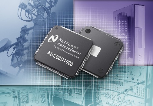
National's ADC08D1000
digitizes two input signals to 8-bit resolution at sampling rates up to 1
giga-samples per second (GS/sec) while consuming 1.6 W from a 1.9-V nominal
supply. By using the fully programmable dual-edge, sampling feature, the product
can achieve 2 GS/sec sampling from one channel by interleaving the two on-chip
converters. Both coarse and fine timing adjustments are available, allowing the
sampling clock for each channel to be calibrated independently in 0.1-picosecond
increments. A three-wire serial bus controls these adjustments, as well as
on-chip functionality, and independent gain and offset fine-tuning for I and
Q-channels. The ultra-low power requirements of the ADC08D1000 enable designers
to eliminate fans or heat sinks, saving board space and reducing system cost.
National's ADC08D1000 is fabricated using the company's 0.18-micron, high-performance CMOS process technology. The device features on-chip auto calibration at power-up that enables low power with high performance. In addition, it has performance-enhancing folding/interpolating architecture. Folding reduces the number of comparators, and interpolation greatly reduces the number of front-end amplifiers required, saving power and reducing the load on the input signal. The ADC08D1000 guarantees "no missing codes" over the full operating temperature range of -40 to 85°C. In addition, the ADC08D1000 features National's LVDS interface, which enables reliable transmission of high-speed signals, while maintaining low noise and distortion levels.
The ADC08D1000 is designed with an extremely low bit-error rate (BER) of 10-18. At a 1 GHz sampling rate, the ADC08D1000 achieves 0.25 least significant bits (LSB) differential non-linearity (DNL) and 0.35 LSB integral non-linearity (INL), while maintaining 7.5 effective number of bits (ENOB) from DC up to input frequencies of 500 MHz (Nyquist). Measured crosstalk between the I and Q-channels is less than -77 dB. The dual on-chip sample-and-hold amplifiers deliver suitable dynamic performance over a 1.7 GHz full power bandwidth.
These products will be followed closely by a 500 mega samples per second (MS/sec) version and National's 1.5 GS/sec device in the first quarter of 2005. All speed grades in National's ultra-high-speed portfolio have the same pin-out, allowing the designer to change the sampling rate without changing the board layout. In addition, National is developing higher-resolution 14- and 16-bit pipeline A/D converters and continuing to build its low-power, general purpose successive approximation register (SAR) A/D converters for broad market applications.
The ADC08D1000, housed in a 128-lead exposed-pad package, is priced at $219 in 1,000-piece volumes. The product is scheduled for full production release in January 2005 and samples will be available at that time.
Linear Technology Corp.
Also in September, Linear Technology Corp.,
Milpitas, Calif., rolled out a new family of high-speed, single-version A/D
converters that combine strong AC performance with low power, making them suited
for a range of wireless and cable communications systems.
The LTC2220 family includes single, A/D converters ranging from 10 mega-samples per second (MS/sec) up to 170 MS/sec at 12-bit and 10-bit resolution, as well as 14-bit converters up to 80 MS/sec with parallel outputs.
With Linear Technology's older LTC1750, 5-V family of A/D converters, customers were more than happy to use regular CMOS level single-ended buffers with a clock rate of up to 80 MS/sec, said Todd Nelson, Linear Technology's product marketing manager for mixed signal products.
However, some customers changed their tune when Linear introduced its high-speed 3-V LTC2220 family of A/D converters. This family includes A/D converters ranging from 10 MS/sec up to 170 MS/sec at 12-bit and 10-bit resolution, as well as 14-bit converters up to 80 MS/sec.
At about 100 MHz, customers began asking if there was something they could do to reduce the noise created by digital switching, Nelson said. Consequently, Linear Technology put LVDS outputs as an optional feature on its 135-MHz and 170-MHz LTC2220 devices, he said. The LVDS output option isn't available on lower speed products since Linear Technology doesn't want to have to double the I/O pin counts, Nelson said. One of the tradeoffs of using this I/O is that it results in twice as many pins, since LVDS requires two pins to every one CMOS pin, he explained.
Linear Technology's 135-MHz version device (LTC2221) with a CMOS-output measures 9mm x 9mm in a 64-pin package, for example, while the LVDS-output device (LTC2224) measures 7mm x 7mm in a 48-pin package.
Not everyone believes performance is everything. Sometimes package size outweighs the overall performance benefit of the converter core. There are 10- and 12-bit resolution 65 MS/sec applications, such as medical imaging where package size and power dissipation are just as important as the signal-to-noise (SNR), said Jon Hall, strategic marketing manager for high-speed converters, Analog Devices Inc., Norwood Mass. "They might sacrifice a couple of dBs in performance for a smaller footprint," he said. Customer premise equipment, like a cable set-top box, are another instance where designers put an emphasis in a smaller package size and are willing to make a tradeoff in AC performance to achieve an overall board space target," he added.
The LTC2220 family of 3.3-V converters feature significantly lower power than competing devices without sacrificing AC performance. These low power A/D converters excel at undersampling, making them suited for communications applications such as WCDMA cellular basestation transceivers, digital predistortion power amplifier linearization, and cable modem termination systems.
At 630 mW, in a 7mm x 7mm QFN package, the LTC2224, 12-bit 135 MS/sec A/D converter, has the lowest power at this speed, is almost half the size of its nearest competitor, yet achieves over 67 dB signal-to-noise (SNR) up to 170-MHz input — better than even higher-powered competitors. Further, the system footprint is small because few external bypasses are needed. Intended for low power basestation designs and optimized for undersampling, the LTC2224 features a 775-MHz bandwidth and achieves 77-dB spurious-free dynamic range (SFDR) up to 250-MHz input. Pin-compatible versions at sample rates of 105 MS/sec and 80 MS/sec feature even lower power. Pin-compatible 10-bit versions at each speed are also in full production.
The entire LTC2220 A/D converter family, which includes 24 devices, will be introduced by the fourth calendar quarter. Linear's new A/D converter family offers pin-compatibility, allowing easy migration from 10-bit to 12- or 14-bits, or to different sample rates. In addition to the LTC2224, Linear has introduced five additional high-performance, low-power A/D converters — LTC2222, LTC2223, LTC2234, LTC2232 and LTC2233. All are now in production and are packaged in 7mm x 7mm QFN packages.
Pricing for the 3-V devices range from between $6.70 for the LTC2233, 10-bit device to $33.92 for the LTC2224, 12-bit device in 1,000-piece quantities.
For an overview of the entire LTC2220 family, including pricing, availability and data sheets visit: http://www.linear.com/
Analog Devices Inc.
Analog Devices Inc. unveiled quad A/D
converters for high-density, space-constrained systems, such as medical imaging
systems — which can require more than 100 converters per system — or
space-constrained, multi-channel applications, such as wireless communications
basestations in October 2003. Using serial LVDS data outputs, Analog Devices is
able to integrate four A/D converters onto a single chip, creating a solution
that is compact, fast, cost competitive, and power-efficient. The LVDS outputs
dramatically reduce pin count, package size, number of board traces, and
substrate noise.
"The demand for increased system resolution and speed is driving the number of ADCs used in these systems higher, so manufacturers are striving to pack more converters into smaller spaces," said Kevin Kattmann, product line director for high-speed converters, Analog Devices, Inc. "The serial LVDS digital outputs allow the new quad ADCs to radically simplify board layout, enabling more data conversion paths to be routed on a board."
The first members of the new AD92x9 quad A/D converter family are the 12-bit 50-/65-MS/sec AD9229, and the 8-bit 65-MS/sec AD9289. Both parts are general-purpose converters for high-channel-density applications.
The AD9229 features 70-dB SNR, 85-dBc SFDR, ±0.3-LSB differential nonlinearity (DNL), and +/-0.6-LSB INL. Operating from a single 3-V power supply, the AD9229 consumes less than 220 mW per A/D converter core.
The AD9289 specifies 49-dB SNR, 70-dBc SFDR, ±0.25-LSB DNL, and ±0.5-LSB INL. Operating from a single 3-V power supply, the AD9289 consumes less than 68 mW per A/D converter core. Both parts deliver the same dynamic performance found in four single A/D converters, while maintaining exceptional channel matching and excellent cross-talk isolation, with virtually no cross-talk over the full operating range.
Although these devices have been available since last October, the company has only been producing prototype quantities, according to Hall. He expects volume shipments to start ramping up in the first quarter next year, he said.
The AD9289 is available in a 64-lead BGA package and is priced at $2.63 per channel in 1,000-piece quantities. The AD9229 is available in a 48-pin 7mm x 7mm LFCSP and is priced starting at $8.50 per channel in 1,000-piece quantities.
Find more information at: http://www.analog.com/en/prod/0,2877,AD9229,00.html#
Texas Instruments Inc.
In February, Texas Instruments Inc., Tucson,
Ariz., introduced eight-channel, ultra-low-power, high-speed A/D converters with
an LVDS interface. The family of octal, 10- and 12-bit, high-speed A/D
converters from the company's Burr-Brown product line feature serial LVDS
outputs and consume 123 mW of power per channel at 65 MS/sec (138 mW/channel at
70 MS/sec). The devices allow high system density in ultrasound, wireless
communications, optical networking, instrumentation, test and measurement, and a
variety of other multichannel applications.
"The innovative ADS527x family offers the highest level of integration and performance by providing eight parallel, 12-bit A/D converters with 70.5 dB SNR at 70 MS/sec. By combining this integration with the lowest power per channel of competitive products, the ADS527x will enable higher channel counts and higher performance in applications such as ultrasound, positron emission tomography (PET) scanners and numerous other imaging and communications systems," said Ed Fullman, product marketing manager for TI's high-speed data converter products. "Ultimately, these devices will allow designers to integrate more channels into smaller, more affordable systems — enabling advanced diagnostics in a broader range of environments around the world."
The ADS527x family includes 40, 50, 65 and 70 MS/sec versions in 12-bit resolution, and 40, 50 and 65 MS/sec versions in 10-bit resolution. All products in this family are both pin and serial LVDS compatible, providing a simple upgrade path in both sample rate and resolution.
Serial LVDS greatly simplifies the A/D converter's interface and allows for compatibility between the different family members in terms of speed and resolution. TI's implementation of serialized LVDS offers the user the flexibility to optimize interface power dissipation based on system requirements, and is compatible with Xilinx and Altera programmable devices.
The integration, performance and power of the ADS527x family will allow imaging systems, such as ultrasound, to improve image quality with exceptional 12-bit, 70.5 dB SNR performance, reduce power requirements, increase channel density and decrease board space demands.
The ADS527x family offers SNR of 70.5dB (60.5 dB for the 10-bit family) at 10-MHz input frequency. The devices provide internal references to simplify system design requirements, or can be driven with external references. The ADS527x family operates from a 3.3-V supply.
All eight channels share a common sample clock for excellent skew and jitter performance. Individual power down of each A/D converter channel enables optimized operation. A peak-to-peak differential input range of 2 V maintains signal integrity, and a common internal or external voltage reference allows excellent matching between channels.
The devices are packaged in an 80-lead TQFP. Pricing ranges from between $32 for the ADS5275, 10-bit, 40 MS/sec converter to $121 for the ADS5273, 12-bit, 70 MS/sec in 1,000-piece quantities.
Maxim Integrated Products
Maxim Integrated Products, Sunnyvale,
Calif. unveiled the MAX1126/MAX1127 high-speed A/D converters in March. These
A/D converters feature four high-performance, low power, 12-bit A/D converter
cores integrated into a single, space-saving package. These ICs are targeted at
high-channel-count applications that can have as many as 512 A/D converter
channels and require both high performance and low power. Typical applications
include medical imaging and wireless communication.
To address the demanding power constraints of these applications, the MAX1127 consumes less than 140 mW per channel at a sample rate of 65 MS/sec. The MAX1126 consumes only 130mW at 40 MS/sec. Both products offer 69 dB SNR.
To address high-density requirements, the MAX1126/MAX1127 offer a choice of either a serial, LVDS interface or a scaleable low-voltage signaling (SLVS) interface. The serial LVDS/SLVS interface significantly reduces the pin count, thus reducing package size and board trace clutter. Unique to the MAX1126/MAX1127 is a self-aligning data-clock to data-output interface, which greatly simplifies the timing interface for the user.
The MAX1126/MAX1127 are available in a small, 68-pin QFN-EP package specified for the industrial temperature range. Prices for the MAX1126 start at $31.85 and $35.85 for the MAX1127 (1000-up, FOB USA). An evaluation kit is available to speed designs.
Intersil Corp.
Intersil Corp., Milpitas, Calif., revealed that it
will soon be added to the list of A/D converter makers using LVDS. These
products are under development, according to the company.
Parallel Versus Serial LVDS Outputs
TI, Analog Devices and Maxim
offer A/D converters with serialized LVDS outputs. Demand for serialized A/D
converters is being driven by multichannel-type applications like ultrasound,
medial imaging, portable hand held measuring equipment, portable test equipment
and some communications applications.
Ultrasound systems, for example, require anywhere from 64 to 512 channels per system. With a serialized A/D converter, four converters can fit in the same footprint as one converter. This reduces board space, simplifies routing, signaling and lowers power, explained ADI's Hall.
The wireless infrastructure marketplace is discovering multichannel high-speed converters with either integrated A/D converters and D/A converter blocks, or just multiple A/D converter blocks. They've found that in some parts of the world, picocells or very small basestations are needed to take care of hot spots, where capacity is peaking at certain times of the day. Instead of building another million dollar cellular basestation, they are able build picocells, which utilize multichannel high-speed converters, Hall said.
In wireless communications systems, such as basestations and picocells, serial A/D converters can help improve system performance by reducing system complexity, handling more voice channels, reducing system form factors, increasing flexibility and lowering operating costs.
Space constraints and overall system power are two factors driving multichannel high-speed converter use in picocells. Also the price point for these multichannel converters is changing the way they partition the radio, Hall said. There used to be one A/D converter per input carrier. Then they went with a high performance A/D converter to support multiple channels per A/D converter. This A/D converter price was higher but it supported more carriers. The picocell is generally a single carrier platform so the A/D converter performance is not as stringent as the multicarrier platform, and OEMs can fall back to allocating one carrier per A/D converter. So a quad could support two carriers (another aspect of the radio platform is main and diversity) for future growth or partition the picocell sectors into fourths or eighths. Each sector would support one carrier (main and diversity). Splitting into four sectors would require two quad A/D converters. Otherwise, using the same partitioning the radio would have eight single A/D converters, hence taking up more board space. The price of a quad is considerably less than the price of four single A/D converters, as well as two high performance A/D converters that would solve the same issue via a multi-carrier configuration, Hall said.
Power Dissipation and Serial Outputs
In the past, power
dissipation has been a concern when serializing LVDS, because the serializing
process could potentially increase power. When taking multiple LVCMOS signals
and reducing them to one or two LVDS signals, for instance, the signal reduction
may require more power than what is currently being consumed.
However, technology advancements in the A/D converter core, are removing this concern. Moving from smaller geometry's — from .5 micron CMOS to .35 micron CMOS to .18 micron CMOS, is allowing power dissipation in the A/D converter core to decrease. The supply voltage and geometry size of the processor are both shrinking so you can get the same kind of performance with less power consumption, explained ADI's Hall.
Five years ago, a 12-bit, 65 MS/sec parallel output A/D converter would consume 500 mW of power. Today, total power consumption for ADI's quad A/D converters is equal to what one A/D converter would consume five years ago, because of these technology achievements, Hall said. Even though ADI took a hit in the LVDS driver, with increased power consumption, the total aggregate power consumption is still a net gain, he said. "Essentially, our quads today are close to 700 mW and we have generations that will break the half-watt target for the next-generation of multichannel A/D converters. Probably within the next nine months, per A/D converter will consume less than 100 mW per channel," Hall said.
TI Reveals Forthcoming ADCs With Embedded Clocking
TI plans to be
the first to market A/D converters that utilize LVDS that include an embedded
clock and 8B/10B encoding, according to Fullman. TI's yet to be announced
serialized LVDS A/D converters utilize a SERDES approach. Essentially, embedding
clocking into the serial stream reduces the number of interface signals. Instead
of having an explicit clock and explicit frame to define the boundaries of the
word, all of that information will now be embedded into the serial stream,
Fullman explained. With only one serial stream and no explicit clock or explicit
frame, this will become the simplest of all interfaces from a layout
perspective, Fullman said. The A/D converters will also offer pin compatibility
between different resolutions and speeds.
While TI's multichannel ADS5270 A/D converters with the explicit clock were designed with ultrasound applications in mind, the embedded clock format will be of most benefit to the communications market, such as picocells and radios, Fullman said.
Pressing the power consumption and sample rate boundaries and providing the industry with unheard of bandwidth swallowing capabilities has caused some problems, Fullman said. Wide bandwidths and high sample rates mean more data has to be transferred. Solutions have been many, ranging from multiple-de-interleaved CMOS outputs, to utilizing LVDS to create a single high-speed serial or parallel interface. In the most popular sample rates, the serial link seems to provide users with the most advantages, Fullman said. Several forms of the serial interface are being considered for integration into high-speed A/D converters. The explicit clock format is already on the market. TI's ADS527X family has this capability. The explicit clock format dictates that each A/D converter transmits its own data, serialized on a single LVDS pair. To demark the middle of the data window, the data clock must also be provided in LVDS format. And finally, to identify the boundaries of the words, a separate word clock must be generated as well. Together, these signals provide all the information necessary for a receiver to capture the A/D converter bit streams. This format is particularly useful in high channel count systems. An alternative format is to embed the clock into the data stream. Doing this requires that additional bits be inserted into the bit stream with specific values. A PLL in the receiver then looks for these specific bit patters and locks onto those, thus extracting both the data clock and the word boundaries from the single incoming bit stream. The advantage of using this method is that the interface signals are reduced. The disadvantage is the overhead associated with embedding the clock. Further overhead is typically added to provide error correction capability, and to guarantee that the PLL lock patter is truly unique, Fullman explained.
Other A/D converter makers, however, aren't as keen as TI to embed the clock, even though FPGA makers seem to be pushing for this to happen since their devices support 8b/10b coding, which is used frequently with LVDS in Ethernet applications.
"Embedding high-speed clocks within the LVDS signal can cause problems for designers who are working on the receiving end of the signal," said Leonardo Azevedo, National Semiconductor's product marketing manager for high-speed A/D converters. "National has a lot of experience using 8b/10b coding on LVDS streams on interface devices. However, we still have customers asking us to keep the clock external."
Analog Devices echoed a similar statement. While ADI has integrated serial clocks on its LVDS A/D converter roadmap, the company doesn't perceive that the market has warmed up sufficiently to this feature as of yet, Hall said. "Furthermore, there are costs associated with integrating the clock — the level of complexity increases on both sides (converter and digital ASIC) since there would be clock generation and clock recovery blocks required in the respective chips. But at ADI, we anticipate and respond to market demand — so stay tuned," he added.
Company Contacts:
Analog Devices Inc.
http://www.analogdevices.com/
Phone:
1-800-Analog-D
Intersil Corp.
http://www.intersil.com/
Phone: (408)
935-4300
Linear Technology Corp.
http://www.linear.com/
Phone: (408)
432-1900
Maxim Integrated Circuits
http://www.maxim-ic.com/
Phone:
1-800-998-8800
National Semiconductor Corp.
http://www.national.com/
Phone: (408)
721-5000
Texas Instruments, Inc.
http://www.ti.com/sc04020
Phone: (972)
644-5580
Copyright 2003 © CMP Media LLC