11/14/2000
DC Specifications of ADCs and
DACs
Part 1: Basic Tests
By Jerry Horn
The "DC" specifications for analog-to-digital converters (ADCs) and digital-to-analog converters (DACs) are of extreme importance in many applications. Unfortunately, the numbers can be very confusing, and there is a lot of variability in their definitions from manufacturer to manufacturer (and even with a single manufacturer). This column attempts to define the basic equations that govern most DC specifications and to describe how a data converter is tested in order to determine its DC performance.
The basic DC tests for ADCs and DACs include offset error, gain error, differential nonlinearity (DNL), and integral nonlinearity (INL). Depending on the type of converter, the gain error may be replaced by two specifications that are typically called positive full-scale error and negative full-scale error. For ADCs, an additional specification is "no missing codes." For DACs, there is a similar specification called monotonicity. Both of these specifications are directly related to the converter's DNL.
I find it difficult to discuss DC specifications without also describing the test setup that is used to measure the device's performance. For an ADC, the hardware requirements include a servo-loop circuit for the device under test (DUT) and a high-resolution digital voltmeter (or digital multimeter) with a minimum of 6½ digits of resolution, with 8½ digits preferred for high-resolution converters. For DACs, only the voltmeter is needed.
In the case of ADCs, the underlying purpose of the servo-loop circuit can be difficult to grasp at first. For the following discussion, assume that the goal is to measure the voltage at an ADC's input where the converter's output code toggles evenly between two adjacent codes. The most recent output code of the ADC will be called K and the desired "target" codes will be called J and J+1.
Thus, the servo-loop circuitry accepts a target code J and servos a "DC" (or very low noise and very stable) analog input voltage to the DUT until the output code K is distributed evenly between J and J+1. In reality, the servo loop adjusts the analog input voltage until J or any lower code is produced approximately 50% of the time, and J+1 or any higher code is produced the remaining 50% of the time (or so). When that point is reached, the analog input voltage will be precisely at the point (within some margin of error) where the output code transitions from J to J+1 (see Figure 1).
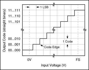
Figure 1 - Transfer Function for a
Linear N-bit Unipolar ADC
Note that if code J or J+1 is missing, the proper voltage will still be produced unless code J is 0 or code J+1 is 2N - 1 (where N is the resolution, in bits, of the ADC). If either of the two end codes is missing, the servo loop will produce the wrong voltage (the servo loop circuit will "rail"). This particular observation is very important in the operation of the servo-loop circuit: it works even if J or J+1 is missing unless J = 0 or J+1 = 2N - 1.
In a sense, the servo-loop circuit is used to make an ADC into a DAC. When running a DC test on a DAC, the desired code J is simply fed into the DAC and the output voltage is measured (see Figure 2). By compiling an array of voltages for each code, all DC specifications can be calculated. Likewise, an ADC and a servo-loop circuit work together to form a similar arrangement: the target code J is fed into the circuit, which results in an analog voltage being produced. When the voltage at each code transition has been measured, the resulting data can be used to compute the DC specifications.
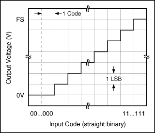
Figure 2 - Transfer Function for a
Linear N-bit Unipolar DAC
Unfortunately, the result in these two cases is not exactly the same. If you compare Figure 2 to Figure 1, you will notice that the transfer function of the ADC is slightly different than the transfer function of the DAC. The DAC input is discrete and the analog voltage jumps with each code. For the ADC and servo-loop circuit combination, the input voltage is continuous, but the output code is discrete. The servo loop allows the transition point between two codes to be located, and this voltage is ½ of a least significant bit (LSB) from the code "middle."
Ideally, there would be a way to find the voltage that produces the middle of each step in the ADC's transfer function, rather than the transition point between two codes (called the "code edge" or "code transition"). This would allow the computations for an ADC's DC specifications to be identical to those for a DAC. In fact, for those ADCs whose output codes span many LSBs with low noise and a stable DC input, it is possible to find the middle of the code. For example, a 24-bit industrial ADC could be tested in this manner. Some 16-bit, 100 kHz ADCs could also be tested in this way, while other 16-bit, 100 kHz ADCs could not. For all ADCs, the code middle can never be found for codes 0 and 2N - 1.
As far as I am aware, even for those ADCs where the code middle could be found, the typical test technique involves finding the code edge. The circuitry and algorithms for doing this are simpler than for finding the code middle, and are consistent with those the techniques used for ADCs where the code middle cannot be found (such as a 12-bit, 100 kHz industrial ADC). So, this means that the calculations associated with DAC DC testing are different than those for ADC DC testing.
In order to accomplish the DC testing, a computer is required in addition to the voltmeter (and servo-loop circuit in the case of ADC testing). The computer is used to control the target code and to read the result from the voltmeter. Computer software will then be able to determine offset error, gain error, INL, and DNL.
Note that in regards to INL testing, there are two methods to compute INL: the "end-point" method and the "best-fit" method. The endpoint method relates the INL to a straight line drawn through the end points of the converter's transfer function. The best-fit method relates the INL to a straight line that best fits the transfer function. (Note that the endpoint method can produce results up to two times greater [worse] than the best-fit method, but the best-fit method can never produce numbers worse than the endpoint method. In other words, the endpoint method is the most conservative way to measure a converter's linearity. Thus, the endpoint method is also considered to be a more "honest" measurement.)
DC Specifications for DACs
The basic DC tests for DACs include offset error, gain error, differential nonlinearity (DNL), and integral nonlinearity (INL). The calculations associated with these tests are somewhat easier to understand than those for ADCs, so they will be presented first.
For simplicity, the following discussion assumes a DAC with a unipolar output range of 0 V to VREF (internal or external reference voltage). Some DACs offer a bipolar output range of -VREF to +VREF, or they may provide a scaling factor that scales the analog output voltage by some value. So, the actual output range might be from 0 V to SF × VREF, -(SF × VREF) to +(SF × VREF), or even -(SF × VREF + OF) to +(SF × VREF + OF) where SF is a scaling factor and OF is an offset factor.
Rather than complicate the discussion that follows, the definitions of the DC parameters assume a DAC whose output range is 0 V to VREF (technically, it would be VREF minus one LSB; this is also the full-scale voltage, abbreviated "FS"). The transfer function for such a DAC is shown in Figure 2. If the actual DAC output is scaled but is still unipolar, the modifications to the equations are trivial. If the output range is bipolar, then the changes are slightly more complicated, but still derive from the basic equation presented here. (The biggest difference for a bipolar DAC is the possibility of defining both a positive full-scale error and a negative full-scale error.)
In the discussion that follows, numbers with a H at the end are in base 16 (hexadecimal) format, N is the resolution of the converter (in bits), VZS is the voltage produced by the lowest input code (12-bit DAC example: 000H), VFS is the voltage produced by the highest input code (12-bit DAC example: FFFH), VJ is the voltage produced by input code J (example, V0 = VZS and VFFF = VFS for a 12-bit DAC), and 1LSB is the voltage "weight" of an ideal LSB as defined by 1LSB (in volts) = VREF/2N .
Offset ErrorVZS is measured, and this is the offset error voltage. If expressed in LSBs, the offset error voltage is divided by the weight of an ideal LSB.Offset Error (in LSBs) = VREF/ILSB Gain ErrorVFS is measured. The voltage of the reference is also measured. From this voltage reading, 1 ideal LSB weight is subtracted, producing an ideal value that represents the full-scale output voltage of the converter. The zero-scale output voltage is measured and is subtracted from the measured full-scale output voltage. The resulting value is subtracted from the ideal voltage span of the converter. If expressed in LSBs, the gain error voltage is divided by the weight of an ideal LSB.
Gain Error (in LSBs) = [VREF - 1 × ILSB - (VFS - VZS)]/ILSB
In addition to gain error, the error at full scale can be expressed as a simple error relative to VREF without taking into consideration the offset error (VZS). In this case, the equation is
Full-Scale Error (in LSBs) = (VREF - 1 × ILSB - VFS)/ILSB
If the output of the DAC is a bipolar voltage around 0 V, then offset error is called bipolar zero error, full-scale error is called positive full-scale error, and an additional error exists at minus full scale, and is called, cleverly enough, negative full-scale error.
Integral Nonlinearity (INL)The input code is initially set to zero scale and the VZS voltage is measured. Then the VFS voltage is measured. The target code is then swept from zero scale to full scale. After each code has been sent to the DAC and the output has settled, the analog result is measured. The INL at that code is
INLJ (in LSBs) = [VJ - (J × ALSB + VZS)]/ALSB ,
where J is the target code, VJ is the measured output voltage, and ALSB is the actual voltage weight of each LSB as computed by the following equation.
ALSB (in volts) = (VFS - VZS)/(2N - 1)
Note that offset and gain error could use ALSB for expressing their respective errors in LSBs, or INL could use ILSB for expressing its error in LSBs. However, the specifications for most DACs imply that gain and offset error are relative to an ideal LSB, while INL and DNL are relative to an actual LSB (note that this is open to some debate). In reality, the difference between ALSB and ILSB is typically very small.
The definition that has just been provided for INL relates the value of each individual code to the end-point voltages, and is referred to as the endpoint method (compared to the "best-fit" method). Also, the INL for the zero-scale code and the full-scale code is zero when using the endpoint method.
Differential Nonlinearity (DNL)The target code is initially set to zero scale, and VZS is measured. Then VFS is measured. The target code is then swept from zero scale to full scale. After each code has been sent to the DAC and the output has settled, the analog result is measured. The DNL at that code is
DNLJ = [(VJ - VJ-1)/ALSB] - 1 ,
where J is the target code, VJ is the measured voltage at code J, VJ-1 is the measured voltage at code J-1, and ALSB is the actual voltage weight of each LSB as computed by the following equation.
ALSB (in volts) = (VFS - VZS)/(2N - 1)
See the INL discussion for comments regarding ILSB vs. ALSB. Note that DNL is computed in the same manner regardless of which INL method is used (endpoint or "best-fit"). Also, the DNL for the zero-scale code cannot be measured.
DC Test Example for a DAC
Figure 3 shows an example of the DC test
results for a 16-bit DAC. Note that this converter is extremely
linear for a 16-bit device. Also, because this converter offers a bipolar
output, there are three key errors: offset, positive full-scale, and negative
full-scale.
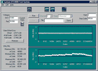
Figure 3 - DC Test Results for a 16-bit
DAC
DC Specifications for ADCs (measured with a servo-loop setup)
For simplicity, the following discussion assumes an ADC with a unipolar input range of 0 V to VREF (internal or external reference voltage). Some ADCs offer a bipolar input range of -VREF to +VREF, or they may provide a scaling factor that divides the analog input voltage by some value. So, the actual input range might be from 0 V to SF × VREF, -(SF × VREF) to +(SF × VREF), or even -(SF × VREF + OF) to +(SF × VREF + OF), where SF is a scaling factor and OF is an offset factor.
Another possibility is that the converter may be specified such that the offset error and the gain error are calculated directly from the transition points at each end of the ADC's transfer function. Normally, the voltage that is produced by the servo-loop setup is adjusted by ½ of an LSB (see Figure 1). However, this is not always the case. In addition, some calculations for offset error and gain error take into account the measured value for the LSBs near each respective end point. This can produce more accurate results for converters that are not very linear.
Rather than complicate the discussion with the many different possibilities, the definitions of the DC parameters assume a fairly linear ADC whose input range is 0 V to VREF and whose offset error and gain error results are offset by ½ an LSB from the actual meter reading. If the actual ADC input is scaled but is still unipolar, the modifications to the equations are trivial. If the input range is bipolar, then the changes are slightly more complicated, but still derive from the basic equation presented here. (The biggest difference for a bipolar ADC is the possibility of defining both a positive full-scale error and a negative full-scale error.)
In the discussion that follows, numbers with a
subscript H at the end are in base 16 (hexadecimal) format, N is the resolution
of the converter (in bits), VZS is the voltage that produces the transition
between the zero-scale code and the next highest code (12-bit DAC example:
000H and 001H), VFS-1 is the voltage that produces the transition between
the full-scale code minus one and the full-scale code (12-bit DAC example:
FFEH and FFFH), VJ:J+1 is the voltage that produces the transition between
code J and code J+1 (example, V0:1 = VZS and, for a 12-bit converter, VFFE:FFF
= VFS-1), and ILSB is the voltage "weight" of an ideal LSB as defined by
1LSB (in volts) = VREF/2N .
Offset ErrorVZS is measured. From this voltage reading, ½ of an ideal LSB "weight" is subtracted, producing the value of the zero-scale voltage. This is also the offset error voltage. If expressed in LSBs, the offset error voltage is divided by the weight of an average LSB.Offset Error (in LSBs) = (VZS - 0.5 × ILSB)/ILSB
Gain ErrorVFS-1 is measured. The voltage of the reference is also measured. From this voltage reading, 2 ideal LSB weights are subtracted, producing an ideal value that represents the input span of the converter from the zero-scale transition to the full-scale minus one transition. The actual zero-scale transition voltage is measured and is subtracted from the measured full-scale transition voltage. The resulting value is subtracted from the ideal voltage span of the converter. If expressed in LSBs, the gain error voltage is divided by the weight of an ideal LSB.
Gain Error (in LSBs) = [VREF - 2 × ILSB - (VFS-1 - VZS)]/ILSB
Integral Nonlinearity (INL)The input code is initially set to zero scale and the VZS voltage is measured. Then the VFS-1 voltage is measured. (The case of a missing code at full scale is not handled with this test algorithm. The servo loop will "rail" if the full-scale code is missing.) The target code is then swept from zero scale to full scale. When each code transition has settled, the input voltage is measured. The INL at that code is
INLJ (in LSBs) = [VJ:J+1 - (J × ALSB + VZS)]/ALSB ,
where J is the target code, VJ:J+1 is the measured transition voltage between code J and J+1, and ALSB is the actual voltage weight of each LSB as computed by the following equation.
ALSB (in volts) = (VFS-1 - VZS)/(2N - 2)
Note that offset and gain error could use ALSB for expressing their respective errors in LSBs, or INL could use ILSB for expressing its error in LSBs. However, the specifications for most ADCs imply that gain and offset error are relative to an ideal LSB, while INL and DNL are relative to an actual LSB (note that this is open to some debate). In reality, the difference between ALSB and ILSB is typically very small.
The definition that has just been provided for INL relates the value of each individual code to the end-point transitions, and is referred to as the endpoint method (compared to the "best-fit" method). Also, the INL for the zero-scale code and the full-scale minus one LSB code is, by definition, zero. The INL for the full-scale code cannot be measured.
Differential Nonlinearity (DNL)The target code is initially set to zero scale, and VZS is measured. Then VFS-1 is measured. (Again, the case of a missing code at full scale is not handled with this test algorithm. The servo loop will "rail" if the full-scale code is missing.) For all-code DNL testing, the target code is then swept from zero scale to full scale minus one LSB. When each code transition has settled, the input voltage is measured. The DNL at that code is
DNLJ = [(VJ:J+1 - VJ-1:J)/ALSB] - 1 ,
where J is the target code, VJ:J+1 is the measured transition voltage between code J and J+1, VJ-1:J is the transition voltage measured between code J-1 and J, and ALSB is the actual voltage weight of each LSB as computed by the following equation.
ALSB (in volts) = (VFS-1 - VZS)/(2N - 2)
Note that DNL is computed in the same manner regardless of which INL method is used (endpoint or "best-fit"). Also, the DNL for the zero-scale code and the full-scale code cannot be measured.
DC Test Example for an ADC
Figure 4 shows an example of the DC test
results for a 12-bit, 100 kHz ADC. Note that this converter has
three missing codes.
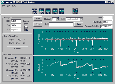
Figure 4 - DC Test Results for a 12-bit,
100 kHz ADC
No Missing Codes and Monotonicity
For an ADC, a particular output code may never
appear regardless of the input voltage. When this occurs, the code is said
to be missing. When performing a DC test on an ADC, a missing code can
be estimated based on the DNL for a particular code.
Assume that a particular 12-bit ADC is missing code 1023 (see Figure 4 for an example). When the target code is 1022, the servo-loop circuit finds the voltage where the converter output toggles between codes 1022 and 1024. At that point, the input voltage is measured (call this voltage X). When the target code is 1023, the servo loop again finds the point where the output codes toggle between 1022 and 1024. This voltage should be the same voltage as was measured previously (call this second measurement Y).
Unfortunately, the two measurements are not exactly the same. Since the DNL computation is
[(Y - X)/ALSB] - 1 ,
the result will not be exactly -1 as it should be. Instead, it will be slightly larger or smaller. Thus, a missing code cannot be determined directly from the DNL data. However, a value very near -1 does indicate that the code has either a very short width or is missing.
To determine a missing code for certain, there must be a definition for "missing code." For example, if the code appears less than one conversion out of every 100 or 1000 that should have produced that code, then the code might be defined as "missing." The exact definition varies. However, this does indicate that the proper way to test for a missing code is to monitor the conversion results. If, over the course of N conversions, the expected output appears less than N/M times (where M might be 100, 200, or 1000), then the code is missing.
It can be argued that the DNL result can be used to determine a missing code. While it can be used to narrow down the possibilities of which codes might be missing, DNL is usually not repeatable enough to determine that a code is, in fact, missing.
As a side note, many programmers will artificially restrict the DNL result to a value of -1 or greater. For a well-behaved ADC, DNL should never be less than -1. However, in some rare cases, it can be less than -1. Also, a value lower than -1 can be used as a quick estimate as to the repeatability of the test setup, the converter's internal noise, and the noise of the test setup.
As with the ADC, a DAC can have a "missing" code (or codes), but it can also have a DNL value less than -1. A missing code would result in no change in the analog output voltage when the input code was increased by one. Because of the way that many DACs are implemented, it's also possible for the analog output voltage to decrease when the input code is increased. There is no limit (within reason) to how much the analog output might decrease, so DNL values significantly lower than -1 are possible. When the DNL for a DAC is less than -1, the DAC is said to be non-monotonic.
A DAC that is non-monotonic is extremely bad for
certain applications. One example is a circuit that controls the physical
position of an item such as a table, robot arm, or cutting head. The circuit
might control the item's position with a DAC and sense the position with
an ADC. Imagine if the item is to be moved slightly by increasing the DAC's
input code by one. If the DAC is non-monotonic at that point, the analog
output voltage will actually decrease. The sensor will indicate that the
item moved the wrong way and the DAC code will again be increased. If the
DAC's output voltage then jumps up suddenly, the item will be too far and
the DAC code will be decreased. The end result will be that the item "chatters"
while continually attempting to reach the desired positionwhich it never
does.
Copyright ©1999-2000 ChipCenter