12/20/2000
DC Specifications of ADCs and
DACs
Part 2: Testing Industrial ADCs and DACs
By Jerry Horn
Part 2 of this series on the DC specifications of ADCs and DACs focuses on how industrial ADCs and DACs are tested in order to arrive at the DC performance of the converter. The DC performance of a converter has important implications in judging the quality of the device as well as predicting the performance of the device for various applications. In some cases, it is also desirable to verify the DC performance of the ADC or the DAC in the actual application. This discussion will address the practicality of such testing.
DAC Test Setup
DC Specifications of ADCs and DACs - Part 1: Basic Tests presented the equations for determining the DC performance of an analog-to-digital converter (ADC) or a digital-to-analog converter (DAC). While the equations are not trivial, they are fairly straightforward once the basic test technique is understood. However, that discussion did not describe the actual test setup in much detail.
The first set of equations that was presented was for calculating offset error, gain error, differential nonlinearity (DNL), and integral nonlinearity (INL) for a DAC. The most basic measurement that must be made for all the equations is the determination of the DAC's analog output voltage for a given digital input code. A block diagram of this very simple test method is shown in Figure 1.
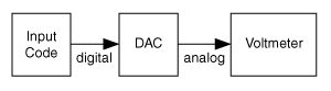
Figure 1 - Block Diagram of DC Test Setup for a DAC
Generally, a personal computer program is written that, via some method, provides the appropriate input code to the DAC. The output of this device is measured by a high-resolution digital voltmeter or multimeter after allowing the DAC output time to settle (this is usually not a problem since voltmeters are very slow relative to most DACs). The result from the voltmeter is read by the computer. This result can be stored into an array that provides the DAC's analog output voltage for each input code, and then the various computations are performed when the test is complete. However, it is also possible to calculate the results as the test is being performed.
There is wide variety of techniques for controlling the input code to the DAC. This can be performed by a simple microcontroller connected to the computer via an RS-232 (serial) port, parallel port, Universal Serial Bus (USB) interface, or General-Purpose Interface Bus (GPIB) connection. It can also be done with a plug-in card that provides for digital output or a vector/pattern generator that can be single-stepped. Of course, there are various trade-offs in regards to cost and test time with each of these methods, and it should be noted there is no one universal technique in common use.
In regards to the voltmeter that is used, any high-resolution voltmeter should be acceptable (I use the term "voltmeter" here, but most of the devices actually tend to be multimeters). Of course, the resolution of the voltmeter should be at least 10 times better than the smallest resolution of the DAC. A 6½-digit voltmeter is generally the bare minimum, and such voltmeters are fairly inexpensivearound $1,000 for a good one with a GPIB interface included.
There is one particular multimeter that many mixed-signal companies seem to preferthe Agilent (formerly Hewlett Packard) 3458A 8½-digit multimeter (lovingly referred to by many as the "macho meter"). This meter is extremely good and is highly recommended. However, it is somewhat expensive at first glancearound $7,000. If you are testing ADCs and DACs on a routine basis, the expense is trivial compared with the benefits of this meter.
Other than the equipment just described and the equations given in Part 1, there is nothing else of significance that is needed to test a DAC for DC performance. Obviously, a test board and a power supply or power supplies are needed, but those are always the most basic requirements of any test setup. Thus, it is possible for a DAC's DC performance to be tested in the end-user's application in a reasonably straightforward manner. (See the suggestions at the end of this document for additional information that might be of help in setting up such a test.)
ADC Test Setup
As was mentioned in Part 1, the test setup for an ADC uses a similar approach to the DAC test setup. In a way, the ADC is turned into a DAC (see Figure 2 and compare it with Figure 1).
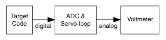
Figure 2 - Block Diagram of DC Test Setup for an ADC
Here again, the equations for calculating the DC performance of an ADC rely on the underlying measurement of the analog voltage that results when the ADC produces a given output code. Specifically, the goal is to measure the analog input voltage that produces a "target code" or lower codes 50% of the time, and higher codes the other 50% of the time. The voltage that produces this condition is called the "transition voltage" for the given target code.
Except for the servo-loop circuit itself and some very minor changes to the overall equations, testing an ADC is exactly the same as testing a DAC. Unfortunately, the servo-loop circuit itself is not trivial.
The Basic Analog Servo-Loop Circuit
The basic analog servo-loop circuit that is used for the DC testing of ADCs is essentially an integrator that integrates up or down depending on the ADC result (see Figure 3). This circuit includes both the target code block and the voltmeter block from Figure 2, as well as more detail about the servo-loop circuit itself.
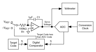
Figure 3 - Basic Analog Servo-Loop Circuit
As shown in Figure 3, a stable, low-noise reference (VREF) provides a current source for the main integrator. When connected to VREF, the output voltage of the integrator decreases. A negative reference (usually an inverted version of VREF) provides the current source to make the integrator voltage increase. (It's also possible to use a real current source or sink, but the circuit still works in the same way.)
The operation of the servo loop is very straightforward. If the target code is less than the most recent ADC output result, then the integrator output voltage is decreasing (integrator input switched to VREF). This will cause the ADC output code to decrease (this discussion assumes a simple straight binary output coding for the ADC where a lower input voltage will result in a lower output code). If the target code is greater than or equal to the ADC output code, then the integrator input is connected to -VREF, and its output voltage increases.
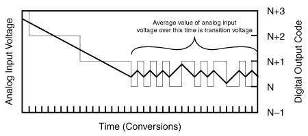
Figure 4 - Integrator Output Voltage Servos to Code N/(N
+ 1) Transition Voltage
Figure 4 shows an example of the servo-loop circuit of Figure 3 settling to the transition voltage between code N and N + 1. As can be seen, the output voltage of the integrator is ultimately a sawtooth waveform whose average value over a given time period is equal to, within some margin of error, the desired transition voltage. Note that both the ADC's internal noise and external noise will somewhat vary the ADC's output code so that the integrator output will not always be stepping back and forth across the transition voltage on every other conversion result (this effect is highly exaggerated in Figure 4the variation of the integrator's output voltage will typically be much smaller than shown).
The values for capacitor C1 and resistor R1 shown in Figure 3 must be such that the variation of the integrator's output voltage is small enough for the voltmeter to measure the transition voltage to the desired repeatability. R1 and C1 must be chosen to work in conjunction with the ADC's conversion rate, its input voltage range, the voltmeter integration time, and the desired test time.
The basic analog servo-loop circuit has several drawbacks for general ADC testing. For one, it can require a great deal of time to servo across the ADC's entire input range. For example, consider a 12-bit ADC. If the servo loop is currently "sitting" between codes 0 and 1, and the test requires a measurement of the transition voltage between codes 4094 and 4095, then the servo loop must slew across the converter's entire input range. Given that the integrator should not change too rapidly over any single conversion period, it may take many tens of thousands of conversion periods for the servo-loop circuit to complete its journey.
In some cases, particularly when testing only a few ADCs or when simplicity is the key, the basic analog servo loop is adequate. The first transition voltage should be given a good deal of time to settle, while others that are nearby will not need nearly the same amount of time. Once the servo loop has settled, each subsequent code can be tested fairly quickly since the servo loop will not have far to go.
Unfortunately, there are times when it is important to re-measure the endpoints during the test. This is mentioned in item 4 under the "Suggestions for DC Testing ADCs and DACs" heading. If the endpoints must be re-measured during the test, the basic analog servo-loop circuit can increase the test time substantially.
In addition, it is difficult to use the analog servo-loop circuit shown in Figure 3 for a wide variety of ADCs or for testing one ADC while varying certain parameters (such as conversion time and reference voltage). Ideally, either R1 or C1 (or both) could be changed to optimize the time constant of the integrator.
An Improved Analog Servo-Loop Circuit
Figure 5 shows an improved analog servo-loop circuit. This circuit addresses both of the problems that have just been discussed relative to the circuit in Figure 3. The improved circuit has a "pedestal DAC" that provides a way to move the analog input voltage to the ADC quickly from one value to another. This gets the input voltage close to the desired value and can be thought of as a "coarse" setting.
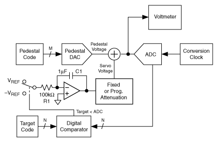
Figure 5 - An Improved Analog Servo-Loop Circuit
The output of the analog integrator is combined with the pedestal DAC voltage to create the input voltage to the ADC. The integrator provides a "fine" voltage via the servo-loop technique that has already been described.
Finally, the output of the integrator is attenuated by an amount that can be fixed or programmable. If fixed, the attenuation can be set manually according to the needs of the particular test being run. If programmable, the value can be adjusted, as previously described, to optimize test time and repeatability for the given device under test (DUT).
Other Servo-Loop Circuits
Another type of servo-loop circuit is a digital servo loop. The integrator circuit shown in Figure 5 is replaced with a DAC (which can be the same type of DAC as is used for the pedestal DAC). The two DACs function as a coarse DAC and a fine DAC. The output voltage of the fine DAC is attenuated and summed with the output of the coarse DAC. Programmable logic or a microprocessor is used to adjust the coarse and fine DAC in order to arrive at the transition voltage. The control logic or algorithms can be fairly simple or quite complicated.
Many such variations of the basic analog servo-loop circuit exist. They all attempt to perform the same function, but use different methods to optimize a particular goal such as reducing test time or improving repeatability without increasing test time.
Suitability for End-User
Unlike a DAC, it is often extremely difficult for the end-user to test an ADC's performance in their particular application. The most common way to implement a test is to use the basic analog servo loop shown in Figure 3 along with programmable logic or microprocessor that are already present in the design. In this case, the slow settling time of the servo-loop circuit is not terribly important because the test will not be performed very often.
For example, the test may be performed manually on only a certain number of output codes. The goal is simply to verify that the converter is functioning reasonably wellno missing codes and no major INL problem.
Suggestions for DC Testing ADCs and DACs
1. Turn off the front-panel display of the voltmeter. This can decrease the total test time substantially as the meter's microcontroller does not have to refresh the display continually. On the other hand, provide an option in the software for allowing the display to be on while testingthis can be very useful for debugging.
2. Do not let the meter autorange, but set it to one particular range (for example, the 12 V range on the 3458). When the meter is allowed to autorange, there can be discontinuities when it switches between two different ranges, which can affect the resulting data.
3. Optimize the integration time of the voltmeter's measurement to give the needed repeatability and accuracy without wasting too much time making a measurement. This is where the Agilent 3458A really outperforms the competition (it is possible to make reasonable measurements on low-resolution devices of 10 bits or less with an integration time as low as 0.01 line cyclesother voltmeters have difficulty maintaining higher resolution results with such a low integration time).
4. If the device is drifting significantly over the time frame of the test, then the INL will not be repeatable. For most ADCs and DACs, the item most likely to drift and cause problems will be the reference. If it cannot be made more stable, then the endpoints of the device must be retested often enough to keep the drift from significantly affecting the results. Also, in this case, calculating INL during the test is much easier than waiting until the end.
Issues Concerning an Analog Servo Loop
1. If both VREF and -VREF are derived from the same source, it is not critical that the reference voltage be perfectly stable. However, it should be fairly low-noise so that the voltage at the ADC input is low-noise. The lower the noise, the more repeatable the measurement. If the noise is too high, the integration time of the voltmeter can be increased to make a more repeatable measurement, but this comes at the expense of test time.
2. If -VREF is derived from VREF by inverting it with an op-amp, offset drift of the op-amp is not typically a concern. If the VREF/-VREF ratio changes too much, the measurement will change and will not be as repeatable. However, nearly all op-amps will be more than adequate for the task.
3. Because of the "glitching" caused by the ADC's sample-and-hold, the voltage obtained by the ADC may not match the voltage that is being measured by the voltmeter. Keep in mind that high-resolution voltmeters are integrating their input voltage (continuous in time), while the ADC is capturing only a brief sample of its input voltage (discrete in time). The two results might not match, and the difference between the two may vary over the converter's input range. In this case, the results will be in error. Use an accurate and high-speed op-amp to keep the two voltages as similar as possible (accuracy and high speed are generally at odds with each other, making it very difficult to choose a good op-amp for the job in some cases).
4. The settling time of the servo loop will be a major concern for DC testing of ADCs, much more so than for DAC testing. However, the main issue is when the servo loop is not already at a nearby code and must slew a significant amount in order to find the transition voltage.
Limitations of the DC Specifications of ADCs and DACs
The DC specifications for most ADCs and DACs provide a great deal of information about the performance of the converter. However, it should be noted that the DC specifications are only applicable for the exact conditions under which the device was tested. That is, the specifications apply when doing many conversions with a stable input driven by the same op-amp used in the original test setup. All of this is in addition to the test conditions outlined in the device's datasheet.
In reality, the DC specifications represent the very best that can possibly be achieved with a given ADC or DAC. All other applications will result in slightly or significantly reduced performance. For some applications, the difference between the DC specifications and the actual performance will be of great importance when choosing a particular device. Here are some concerns.
1. The DC specifications for an ADC do not represent the performance of its sample-and-hold. At higher input frequencies, the ADC's INL will begin to suffer. This is covered in a previous column, The Relationship between Harmonic Distortion and Integral Non-Linearity.
2. The transition noise of an ADC or the output noise of a DAC is not described by the device's DC specifications. The test method for arriving at the DC performance of a converter is inherently averaging, which makes the converter's noise of almost no importance. However, for many applications, noise is a very important specification, particularly when using converters with a resolution of 16 bits or more, or for higher speed converters with lower resolution. For ADCs, this is covered in the column Internal Noise in High-resolution Analog-to-Digital Converters.
3. For DACs used in waveform synthesis applications, the DC specifications can be of little use other than as a rough estimate. Of more importance is the settling time and the glitch energy. Even these specifications are often not complete enough to fully predict performance.
4. It's possible, though unlikely, that an ADC with good DC specifications may have some unusual problems. For example, it might occasionally produce a result that is not within the device's normal output distribution (for more information, see Non-Gaussian Noise Distributions in High-resolution Analog-to-digital Converters). In some cases, this might be a layout problem or inadequate bypassing. However, it is possible for the device to simply have a design flaw that is hidden by the inherently averaging nature of DC testing. See the column Undocumented Problems with Analog-to-Digital Converters for more information about unusual problems with ADCs.
Copyright ©1999-2000 ChipCenter