01/18/2001
DC Specifications of ADCs and
DACs
Part 3: The Error Budget
By Jerry Horn
Part 3 of this series on the DC specifications of ADCs and DACs focuses on the relationship between these specifications and the error budget, which is an estimate of the performance required for a given application. The error budget is often the first step in choosing possible ADC and DAC candidates from the ever-growing list of such devices on the market. An error budget can sometimes include devices that should not be considered or throw out devices that should. This discussion focuses on how the error budget and the DC specifications of an ADC or DAC are related.
The term "error budget" has a fairly loose definition. It some cases, it implies that a particular device must perform at a certain level (the "error budget" for a particular component) or better; in others, it refers to the target performance of the entire application. For this discussion, the term will generally refer to the former and, more specifically, to the desired performance of any analog-to-digital converters (ADC) or digital-to-analog converters (DACs) that will be used in the final application. However, it is critical to have a goal or constraint in mind in regards to the overall application. The converter's calculated error budget must therefore be less than or equal to the total error budget of the final application.
Rather than discuss the issue in generalities, let us consider an example. Assume that a handheld infrared (IR) thermometer with a digital readout is to be developed. In order to digitize the output of the IR temperature sensor, the first thing that must be known is the maximum output range of the sensor. Then, the desired resolution of the digitized result must be determined. A good example would be to measure a temperature range of -50°C to +2,500°C to a precision of 1°C.
In reality, this turns out to be a very demanding task. However, let us assume that the temperature sensor is precise to 0.1°C and that the output of the sensor can be level-shifted and amplified as needed to fit the input range of whatever ADC is ultimately selected. Neither of these items will be true, but it will allow this discussion to focus on the converter.
The discussion that follows is not exclusive to ADCsthe error budgeting process for DACs is very similar. Where there are differences, they will be noted.
Determine an Overall Goal
From the example, the goal of the system is a precision of 1 part in 2550. First, note that the precision of the system is not the same as the accuracy. Precision means the repeatability of the system. If the thermometer is pointed at an object, it should give the same reading as long as the temperature of the object has not changed. However, the reading may or may not be accurate to 1°C.
Many systems are much more precise than they are accurate. In some cases, the goal may be to have the two items equal. However, you can never have more accuracy than precision. In general, all of us seem to like precision even though it may not relate directly to accuracy. Having more digits on a thermometer may result in more units being sold than a competing unit with fewer digits, even if the latter offers better accuracy.
There are definitely applications where precision is more important than accuracy. It may be more important to observe that a change has occurred than to know the actual values involved. In regards to temperature measurement, I believe that accuracy is generally as important as precision, but I also observe that most commercial units appear to offer precision that is better than the accuracy. For the example being presented here, we will focus on both precision and accuracy, but will begin by considering just the desired precision of the thermometer.
So far, we know that the ADC needs to be precise to 1 part in 2,550. Unfortunately, ADCs are not generally specified in this manner. DC specifications are typically in terms of LSBs. Either of these numbers can be translated into the other, but then it is difficult to compare "1 part in 2,550" to "1 part in 4,096" or LSBs where the ADCs have different resolutions.
I believe the best specification for comparison purposes is actually percent of full-scale (%FS or simply %). The overall linearity for many DACs is specified in such units. The equations for converting from "N parts in M" and "LSBs" are given below.
Value (%FS) = (N/M) × 100, for N parts in M
Value (%FS) = (LSBs/2N) × 100, where N is the resolution
of the converter
The goal of the IR sensor digitizer is to achieve at least (1/2550) × 100 = 0.039%FS of performance. A 12-bit ADC with an overall integral nonlinearity (INL) of ±1 LSB has a performance of ±(1/4096) × 100 = ±0.024%FS.
At this point, things can get confusing. The goal of the ADC is to achieve "1 part in 2550" or 0.039%FS of performance. However, most ADCs are rated in terms of "plus or minus" this or that (such as ±0.024%FS). The main concern is the meaning of "1 part in 2550." If the thermometer should display 1000.0°C, then is a reading between 999.0°C and 1001.0°C acceptable, or must it be between 999.5°C and 1000.5°C?
If the exact meaning of "1 part in 2,550" is actually "precise to within 1 part in 2,550," then the specification is ±0.039%FS. If the meaning is really "precise to a range no larger than 1 part in 2,550," then the specification would be ±0.20%FS, one-half of the previous specification. In this case, the performance requirement might be better labeled "±1 part in 5,100." It is critical to make sure that everyone (particularly the marketing people) agree on the definition and what it means in regards to the final application.
As an example, consider the implication of the ±1 part in 2,550 specification when the temperature reading should be 999.9°C. If the current reading is 999.0°C and the temperature increases slightly to 1000.0°C, then the thermometer would be within specification if the temperature reading "jumped" from 999.0 to 1001.0°C. To take this example further, the thermometer would be within specification if it displayed only odd-integer temperature results (1.0°C, 3.0°C, 5.0°C, etc.), assuming that the reading changed when the temperature was precisely in between readings (2.0°C, 4.0°C, 6.0°C, etc.).
Worst-Case vs. Typical Performance
Of course, such performance would not be expected under reasonable and normal conditions. However, it is possible and reasonable for the thermometer to exhibit such behavior over a very small portion of its measurement range. If so, this type of performance should be acceptable by the intended users.
Considering such an extreme situation or even a limited version of it has a direct bearing on the DC specifications of ADCs. All ADCs offer typical performance, which will be better, sometimes far better, than the DC specifications would indicate. This creates an issue that is difficult to address in the context of the error budgetworst-case numbers can be used or typical numbers can be used.
This issue concerns all of the components used in a given design. When analyzing tolerances on passive components in an analog circuit, a worst-case calculation can prove that there is no design that will ever work. However, it is very unlikely that all components will have values that are near their worst-case limits. Instead, a Monte-Carlo analysis can be used along with a root-mean-square (RMS) calculation (as a sanity check) to determine the number of circuits that are likely to fail.
Of course, this estimate must be done with some thought. If the design is made up of many resistors of the same type and value, then it is possible that all devices from one lot might show a similar error relative to their nominal value. This is where engineering judgment and experience proves invaluable. There is no simple, clear-cut method to arrive at a decisionit must be done in the context of the situation and be based on direct experience with the components and circuits in question.
Unfortunately, very few designers have enough experience with ADCs to make a reasonable interpretation of the specifications. Even when the specifications can be "interpreted," it is difficult to justify using a converter whose worst-case specifications might violate the converter's error budget. Thus, worst-case numbers are used when performance is important or critical. On the other hand, there are situations where the worst-case numbers are too conservative.
The ADS7816
Now, let us consider the performance of an actual ADC relative to the desired performance of the thermometer. For no particular reason other than I am very familiar with it, the TI (formally Burr-Brown) ADS7816 will be considered. This is a low-cost ($1 to $2 in quantity), 200 kHz, 12-bit successive approximation register (SAR) ADC. This is probably not the best pick for a thermometer application. It has a higher speed than needed and is possibly more expensive. However, it is very small, very low power, comes in a variety of "grades," and a number of other manufacturers offer pin-compatible versions.
Table 1 compares the INL of the different ADS7816 grades and the desired performance.
Table 1 - Possible Performance Goals and ADS7816 Performance
Item
Maximum Specification(%FS)
±1 part in 2,550
±0.039
±1 part in 5,100
±0.020
ADS7816 Low Grade
±0.048
ADS7816 Grade B
±0.048
ADS7816 Grade C
±0.024
As can be seen, the high grade of the ADS7816 meets the requirements for ±1 part in 2,550, but not ±1 part in 5,100. Such performance will require a higher resolution converter.
The difference between the low grade of the ADS7816 and Grade B lies in the maximum DNL specification (±2 LSB maximum for the low grade, ±1 LSB maximum for Grade B). This raises two interesting questions. How does DNL relate to the error budget? And, how can the DNL be less than -1 LSB? (This last question is answered at the end of this column.)
DNL can be an important consideration, but it does not enter into the type of error budget that is being considered here. The INL specification covers the maximum deviation from "nominal" and, by itself, fully describes the output of the ADC relative to the input signal.
DNL is important in regards to the earlier discussion concerning a slight change in temperature resulting in a reading change of 2°C. For this case, the thermometer was still with the range of ±1 part in 2,550. This is equivalent to an ADC whose INL is ±1 LSB, but whose DNL is ±2 LSB.
It is very unlikely that the DNL specification of a converter will be larger than the INL. In fact, some engineers (who should know better) consider it impossible for DNL to exceed INL. However, this is not the case. It is theoretically possible for the DNL specification to be twice as large as the INL. While I have never encountered this exact case, I have encountered many cases where DNL exceeds INL. Some marketing engineers are so committed to the idea that DNL should be less than or equal to INL that they will increase the maximum INL specification to accommodate the DNL specification.
So, DNL is important to consider when thinking about the maximum "jump" that the converter's output might make in response to a small change at its input. Lower DNL specs indicate a "better behaved" converter and one more likely to perform even better than its INL might indicate. As I mentioned in regards to "interpreting" a converter's specifications, such interpretation would indicate that the Grade B ADS7816 (max. DNL of ±1 LSB) would be a better pick for the thermometer than the Low-Grade ADS7816 (max. DNL of ±2 LSB), even though they both have the same INL specification.
As a side note to this discussion, many DACs are specified for "linearity" only (which is the same as INL) and will not possess a DNL specification. The linearity specification provides all the information that is needed in regards to the error budget. However, as mentioned, it is still nice to see the DNL numbers.
Errors That Worsen the INL Specifications
In a previous column, Internal Noise in High-Resolution Analog-to-Digital Converters, I looked at the transition noise or output noise specification for higher resolution (> 16 bits) ADCs. This specification attempts to describe the variation in the converter's output code over a number of conversions with a stable, DC input. Thus, transition noise adds directly to (or worsens) the INL error for any given conversion.
In most cases, the general rule of thumb is to add three times the transition noise to arrive at worst-case INL. However, as covered in the column Non-Gaussian Noise Distributions in High-Resolution Analog-to-Digital Converters, the transition noise of the converter may exceed its specification if the layout or bypassing is not adequate.
Transition noise can be reduced by averaging multiple conversions. This topic is covered in the column Reducing Noise and Errors Introduced by the Analog-to-Digital Conversion Process. For a thermometer, averaging multiple conversions might be a requirement. So, averaging would work well in this application, and transition noise would be reduced as a result.
Note that the DAC counterpart for transition noise is output noise. As with transition noise, the output noise can be reduced by filtering the DAC output. The noise also determines, along with the linearity specification, how the DAC output will deviate from the desired output.
There are many applications where the output noise of the DAC is not important. This is also true of transition noise. For many low-speed (< 100 kHz) 12-bit ADCs, transition noise is not critical. However, this is certainly not the case with higher speed or higher resolution converters.
In the column The Relationship Between Harmonic Distortion and Integral Non-Linearity, I obviously covered the connection between harmonic distortion and INL. If the input signal to an ADC is changing rapidly, then harmonic distortion may become an issue with respect to the worst-case INL. For the thermometer example, this would not be an issue. Again, it is possible to ignore the problem for many applications, but certainly not all.
These two considerations result in the following equation for an ADC's (or DAC's) overall linearity error:
Worst-Case Linearity Error = ±(Maximum INL + 3 × Noise + Distortion) ,
where "noise" is the transition noise of the ADC (after taking into account any averaging) or the output noise of the DAC (after filtering). Likewise, distortion is the harmonic distortion of the ADC or DAC for the given input or output frequency. (This can also be thought of in terms of slew-rate limitation, though it is not exactly the same thing.) If the application requires a high degree of confidence, noise may be multiplied by a larger number such as 4, 5, or 6. Note that the three items add directlythis is not an RMS sum.
The Error Budget and Accuracy
So far, the discussion has focused on a simple linearity analysis. Error budgets are normally much more involved than this. For example, if the thermometer must be accurate to 1°C, then many additional considerations come into play. The offset error and gain error of the ADC must be considered as well as the offset error and gain error of the IR sensor and any intermediate signal conditioning circuitry (level shifting, gain, filtering, etc.). Drift over temperature is also important.
However, unlike the linearity considerations, the error budget tends to more straightforward for these items. The main concern is in regards to the type of analysisworst-case, RMS, or Monte-Carlo. In addition, the error budget must take into account any calibration that will be performed on the system. This can throw a very interesting twist into the error budget, one that may be very hard to address.
Among the various calibration issues are the possibility of improving the linearity of the IR sensor, the signal path, or even the ADC. A piecewise linear or look-up table correction is possible, and each will impact the error budget in a different way. How often the calibration can be done will also affect it (only once at the factory, every so many months in order to stay with spec, or even every few minutes for certain components such as the ADC).
For these items, I cannot offer much guidance because the topic is so vast. However, I can offer the following advice in regards to the ADC. Be very careful with the exact definition of an ADC's offset error and gain error. The most common source of confusion is the sign. Fortunately, many offset error and gain error specifications are symmetrical (for example, ±2 LSBs or ±10 mV). Another source of confusion is gain error (which removes the effect of offset error) vs. full-scale error (which does not). Full-scale error may also apply to the "full-scale range" (FSR) of the converter or simply to the converter's "full scale" (which is ½ FSR for a bipolar converter, that is, one whose input is symmetrical around ground, such as ±10 V).
Sadly, the datasheets for many ADCs are lacking the definition of offset error, gain error, and full-scale error. They may also lack the typical performance curves that detail gain error and offset error changes vs. reference voltage, conversion rate, etc. Even if such curves are included, they represent only the typical performance that can be expected, not the worst case.
End-Point INL vs. Best-Fit INL
One very important item remains to be covered. In Part 1 of this series, DC Specifications of ADCs and DACs Part 1: Basic Tests, I briefly discussed INL in regards to "end point" and "best fit." The equations described in Part 1 cover only the end-point method.
For most "industrial" converters (which typically offer conversion rates of a few hundred kilohertz or lower), the INL specification is calculated per the end-point method. However, it is critical to make sure that this is the case. Also, if a high-speed converter is being analyzed for an error budget, keep in mind that most high-speed converters are intended for applications in communications, radar, etc. The INL for these converters is typically calculated per the best-fit method.
The difference between the two methods is easy to describe, but may be difficult to visualize. An end-point calculation is done on each of the converter's codes relative to the end points of its transfer function (the two end points have a linearity error of zero). The best-fit method first computes the linearity error relative to the end points and then attempts to minimize the error by calculating a "straight-line" transfer function that is a better fit to the data.
Both methods are certainly valid. However, best-fit INL will always be equal to or better than end-point INL. Best-fit INL is a better predictor of "AC" performance in applications that are not overly concerned with offset error and gain error. End-point INL is a better predictor when the converter's transfer function will be calibrated (manually or automatically) to conform to a desired range. Such adjustments are typically done at the converter's end points.
This is an important consideration for an error budget. End-point INL may be up to two times larger than best-fit INL. If the application requires one or the other, then the appropriate value should be used. Note that it is not valid to simply multiply best-fit INL by two or divide end-point INL by two in order to translation between them. However, multiplying the best-fit INL by two does produce a worst-case end-point INL number (dividing the end-point INL by two provides a best-case best-fit INL number).
Figures 1 and 2 compare a very simple ADC with essentially perfect DNL, but a broad INL "bow." Real ADC's often exhibit such a bow, though it can be difficult to see when the DNL errors are superimposed.
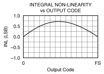
Figure 1 - End-Point INL
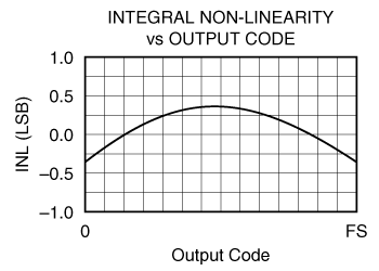
Figure 2 - Best-Fit INL (same converter as Figure
1)
The converter shown in Figure 1 would probably have a maximum INL specification of at least ±1 LSB while the converter of Figure 2 might have a maximum INL of ±0.5 LSB. Note that the converter of Figure 1 could have a maximum INL specification of +1 LSB and -0.5 LSB (or even -0.25 LSB). While this is certainly valid, it is almost never done.
DNL Less (more negative) Than -1 LSB
Previously, I had asked the rhetorical question of how a converter might have a DNL of less than -1 LSB. In regards to a DAC, it is certainly possible for this to occur up to any value of LSBs. See Part 1 of this discussion for more information.
While I did discuss the case of a missing code and also measurement noise in regards to the DNL of an ADC in Part 1 (which might produce a value slightly less than -1 LSB), I did not discuss the case of DNL significantly less than -1 LSB. When the DNL of an ADC is "loosely" said to be -2 LSBs, -3 LSBs, etc., it does not refer to a single code (as it should), but to multiple codes.
For example, if an ADC possesses two missing codes that are adjacent to each other, then the DNL for each code is -1 LSB, period. But, in a sense, the converter has a DNL of -2 LSB (meaning two missing codes that are adjacent to each other). The real location for this information is in the INL results (which will show a delta of 2 LSBs over those two codes). In almost all cases, DNL cannot be less than -1 LSB, but there is some information that is conveyed by knowing that two adjacent codes (or three or four) might be missing.
In regards to "almost all cases," there is a very remote possibility
that an ADC might possess a DNL for a given code that is considerably less
than -1 LSB. This might be the case when an ADC's output code gets "locked"
due to some sort of hysteresis even though the input voltage has changed.
It is very difficult to construct a test for this case and to describe
such performance to the ADC's end-user.
Copyright ©1999-2000 ChipCenter